Transmission circuit design based on signal conditioning chip JHM1101
Transmission circuit design based on signal conditioning chipJHM1101
Haijun Liu, Beijing Jiuhao Micro-ElectronicsCo., Ltd
Abstract: In this article, a cost-effective and high-stability 4-20mA output transmission circuit will be introduced. The main chip adopts the domestic differential signal conditioning chip JHM1101, and the external single op amp is used to build the V/I circuit, which makes the application of the components of the whole circuit has the extremely High flexibility.With digital calibration board and host computer software, single-channel and batch temperature compensation and calibration can be realized when using the chip. This circuit has achieved good results in different applications, and been widely used in the area of measurement of hydraulic pressure, pneumatic pressure and other pressures at present.
Key Words: Pressure Sensor; Signal conditioning chip; Amplifier; Instrument; Sensor
0 Introduction:
JHM1101 is a high-precision analog-to-digital converter designed for differential resistance bridge or half-bridge sensor signals. It can provide digital or analog measurement output signals through a single-wire interface, which providing convenient and accurate measurement results for the sensor. The chip provides both analog and digital output methods, such as rail-to-rail output, 0~1V output, digital signal output and PWM output. It is known that in industrial applications, 4-20mA current is the most commonly used output method. This article describes the method and reference design for applying JHM1101 to achieve this current output.
1 Circuit Structure Design:
The 4-20mA output transmission circuit based on JHM1101 is shown in Figure 1. U2 is the JHM1101 chip, which is directly connected to the Sensor. On the premise that the total working current of Sensor, U1 and U2 are under 3.5mA, this V/I circuit can realize the conversion from voltage calibration output to 4-20mA current output. In order to achieve a small output current, the resistance of RDD and ROUT needs to be in a ratio of 10:1, and the resistance ofRDD should be in the MΩ level. It is recommended that selecting 5V low-power rail-to-rail instrumentation amplifiers for U1, such as OPA337, MCP6001, etc. Zener diode ZD2 provides voltage protection at the VDD side. Q2 is an N-channel JFET used to stabilize the power supply voltage to 5V, which is recommended to choose the MMBF4393. Q1 is the NPN Triode. Considering the withstand voltage and power, it is recommended to choose BCX56 when choosing a model.
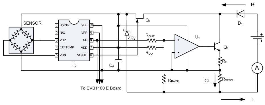
Figure 1. Basic circuit of 4-20mA output transmission based on JHM1101
The output current ICL in Figure 1 is determined by the following formula:

Formula 1.
Defines:

Formula 2.

Formula 3.
Thus the output current can be expressed as:

Formula 4.
It is recommended that each Resistance value in Figure 1. could be: RSENS=50Ω,RDD=1.2MΩ,ROUT=120kΩ,RBACK=24kΩ, Chip's supply voltage: VDD=5V,then Gain=0.2mA,Offset=2mA, which means the formula between output current and voltage is as follows:

Formula 5.
When the expected current output range is 4-20mA, then according to formula 5 the range of VDAC can be calculated as 10%~90%.
Because this circuit uses the back-end current temperature compensation method, the resistance accuracy of RE、RSENS、ROUT、RBACK、RDD can within 1%, and the temperature drift can within 100PPM/℃.
If you want to calibrate the circuit at a single temperature point in order to reduce the calibration cost and prefer to get higher accuracy, it is recommended choosing a low temperature drift resistance within 25PPM/℃ for RSENS、ROUT、RBACK、RDD.
2 Filter Network Design:
To ensure that the input signal is as noise-free as possible, a low-pass filter network is placed between the sensor output and the JHM1101 input pin, as shown in Figure 2.
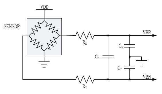
Figure 2. Schematic diagram of low-pass filter network
This input filter has both common mode components and differential mode components. Since the sensor voltage signal is a DC signal, in order to reduce any possible AC noise, the cut-off frequency of this low-pass filter can be set to a very low value.
The cutoff frequency formula definition of this filter:
R6=R7;R0=R6+ RB;C5=C7;C6=10*C5

Formula 6.

Formula 7.
Setting the cutoff frequency of this differential mode filter to fC_DIFF=40HZ can effectively reduce all differential mode AC noise. The cutoff frequency of the common mode filter should be set to Decade at least to avoid converting common mode noise (such as 50HZ noise) into the JHM1101 differential input signal. It is assumed that a ceramic core will be used this time, and the bridge resistance is generally about 10 kΩ, so the value of RB is 10 kΩ. According to the required cutoff frequency of the differential mode filter, the common mode filter capacitor of R6 is ten times that of C5 so only the values of C6 and C5 need to be calculated.
Here C5 takes a capacitor's commonly used value of 10nF, and calculates the value of R6 by the following formula:

Formula 8.
Substituting C5=10nF and fC_DIFF=40HZ into the formula above, the ideal value of R6 is:
R0=18.94KΩ
R6= R7= R0- RB=8.94KΩ
According to this ideal value, the commonly used resistance of 10kΩ can be selected as the standard value. The final cutoff frequency of the filter using R6=10kΩ and C5=10nF is:
fC_DIFF=37.89HZ
fC_CM=1591HZ
In most applications, the low-pass filter cutoff frequency does not need to be very accurate. Therefore, it is enough that the capacitance values of C5、C6、C7 can reach 10% accuracy, and the resistance values of R6、R7 can reach 1% accuracy. In applications which require high precision (for example, requiring a more accurate low-pass filter cutoff frequency) the accuracy of these components can be improved.
3 External protection circuit:
In order to ensure that the module will not be damaged under the extremely harsh environment or by the misoperation of the operator, the external protection circuit is added to the current input and output parts, as shown in Figure 3.
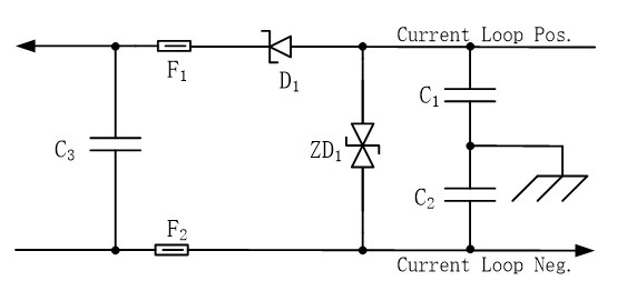
Figure 3. External protection circuit
Two high-voltage low-capacity capacitors C1 and C2 provide a channel for high-frequency interference to the ground, and can also suppress the influence of distributed capacitance. The two magnetic beads F1 and F2 show the high impedance at the critical AC frequency and provide a low DC resistance. The cooperation between C1、C2、F1 and F2 could provide the protection from EMI.
A Schottky diode D1 and a bidirectional TVS diode can provide ESD, EFT and surge protection. D1 guarantees that there will be no current flow through the current loop when the polarity of the power connection is reversed. In this circuit, D1 can choose BAS170WS(or Schottky diodes with similar parameters). This Schottky diode is focus on polarity protection within 70V of voltage. The maximum voltage of the current loop of this module is designed as 30V, so ZD1 uses a bidirectional TVS tube with a breakdown voltage slightly higher than 30V. Note that its leakage current should not exceed 5uA when choosing ZD1, otherwise it will affect the current output results.
The capacitor C3 at the entrance of the circuit is a decoupling capacitor which can ensure that the circuit oscillation will not be caused during the long-line inductive loads.
Capacitance C1 and C2 need to have a high withstand voltage value and a small capacitance value. Therefore, a chip capacitor with a withstand voltage value of 1kV and a capacitance of 10nF could be selected. Magnetic beads F1 and F2 need to have a higher resistance and a low DC resistance value at high frequency. So we choose MMZ1608Y152B magnetic beads for that. TVS diode ZD1 needs: a breakdown voltage slightly higher than 30V, withstanding the instantaneous shock of large current and a response speed within 1nS. Here we choose SMBJ30CA. The choice of C3 should mainly consider the withstand voltage and capacitance value, thus we choose a chip capacitor with a withstand voltage of 50V and a capacitance of 100nF.
4 Principles of Circuit Calibration:
There is always some deviations in the resistance of the resistor in practical applications, so the relationship between the current and the voltage which after increasing the correction deviation is:

Formula 9.
A calibration circuit step needs to be added in the calibration process, the purpose of which is to calculate the ?Gain and ?Offset in the above formula, and then calculate the actual voltage output value in order to finally achieve higher accuracy. The calibration steps are as follows:
①Calculating two theoretical voltage output percentage values based on the current output and the formula in the second section;
②Controlling the DAC output of JHM1101 to output the corresponding percentage of voltage;
③ Collecting the actual currents of the two circuit power terminals respectively;
④Calculating ?Gain, ?Offset;
⑤Substitute the calculated ?Gain and ?Offset into the formula to calculate the actual voltage output corresponding to the current output;
⑥Performing the sensor calibration operation by using the actual voltage output percentage as the expected value of the bridge output.
5 Current's Temperature Compensation Principle:
During the experiment, even if the accuracy of the four resistors-RSENS、ROUT、RBACK、RDD can reach 0.1% and the temperature coefficient could be controlled within 10PPM, the current output signal calibrated using the common front-end compensation method still has a large temperature drift. Because the temperature drift of the current output is related to the temperature coefficient of RSENS、ROUT、RBACK、RDD and the calibration accuracy of the internal R_trim of the JHM1101, it makes it difficult to compensate the transmitter which with a temperature drift less than 0.5% in the full temperature zone. Now using the back-end current temperature compensation method can solve this problem well.
The current’s temperature compensation method can be simply divided into the following four steps to achieve:
① At room temperature, calibrate the 4-20mA signal to obtain the two parameters Gain_B and Offset_B.
② Convert 4-20mA current signal into percentage data.
③ Collect current signals of low temperature and high temperature and transform them into percentage data.
④ Calculate TC_g, TC_o, SOT and other parameters through the calibration algorithm to complete temperature and even second-order compensation.
6 PCB Design:
This design can use a circular double-layer PCB with a diameter of 20mm, as shown in Figure 4.
PCBs of this size are very common in transmitter design, and practical applications can be easily implemented with a little modification. Due to the small PCB size, the placement of the components is relatively close. The JHM1101 may use an internal temperature sensor, so it is placed on the bottom layer with the temperature measuring diode and low-pass filter components, which is the position closest to the Sensor. V/I conversion and external protection components are placed on the top. The actual PCB board is shown in Figure 5.
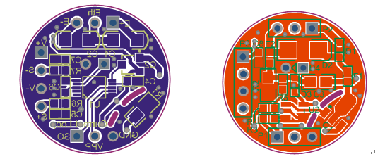
Figure 4. PCB Place & Route
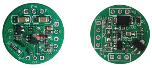
Figure 5. PCB Board
To prevent electromagnetic interference caused by surges, grounding capacitors C1, C2 and ZD1 should be placed close to the current inlet and outlet P2. The traces from the sensor signal to the low-pass filter and JHM1101 input pins should be as short as possible to avoid noise mixed by the analog signal connection. The debugging port connecting line should be far away from the analog signal to prevent the crosstalk. The decoupling capacitors C4 and C8 need to be placed on where very close to the relevant power supply pins. The double-sided large-area copper pour provides a very low ground impedance. The copper pour on both sides of the via can be added in case of need which can reduce the electromagnetic interference generated when the current flows through a single via hole. The heat generated by the internal power consumption of Q1 will cause changes in the ambient temperature. This temperature change will lead changes in the resistance of RSENS、ROUT、RBACK、RDD and the accuracy of JHM1101. Therefore, place Q1 as far away as possible from RSENS、ROUT、RBACK、RDD and JHM1101. It could be found in the PCB layout of [Figure 5. PCB Board] not only Q1 is placed far away from temperature-sensitive components, but also a thermal isolation slot is arranged between them to minimize the impact of Q1 heating on the module's accuracy.
7 Test Results
In conclusion, the design of 4-20mA output transmission circuit based on JHM1101 is completed. In addition, the relationship between the supply voltage and the load is attached (Figure 6). The stable time of the circuit power-on also could be seen in Figure 7.
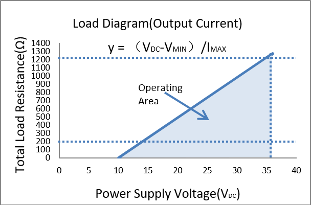
Figure 6. the relationship between the supply voltage and the load
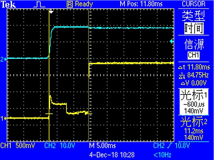
Figure 7. The stable time of the circuit power-on
From this design, more ideal test data can be obtained. The following contents are the test data respectively at 25°C and 85°C after a single temperature point calibration using ceramic piezoresistive cores at 25°C which for the reference:
1)Test Data under 25℃
Pressure (MPa) | Positive stroke output(mA) | Negative stroke output(mA) |
0 | 4.003 | 4.003 |
0.1 | 6.662 | 6.664 |
0.2 | 9.331 | 9.335 |
0.3 | 12.001 | 12.004 |
0.4 | 14.668 | 14.675 |
0.5 | 17.33 | 17.339 |
0.6 | 20.003 | 20.004 |
2)Test Data under 85℃
Pressure (MPa) | Positive stroke output(mA) | Negative stroke output(mA) |
0 | 3.989 | 3.989 |
0.1 | 6.664 | 6.664 |
0.2 | 9.35 | 9.344 |
0.3 | 12.037 | 12.032 |
0.4 | 14.722 | 14.717 |
0.5 | 17.411 | 17.406 |
0.6 | 20.103 | 20.098 |
After testing, with ceramic piezoresistive core in the temperature range of 25~85℃, this circuit can achieve the accuracy within 1% FS (including the temperature drift of the ceramic piezoresistive core), which finally meets the design requirements.
